Company introductionhttps://www.buenooptics.com/
Business item(s)
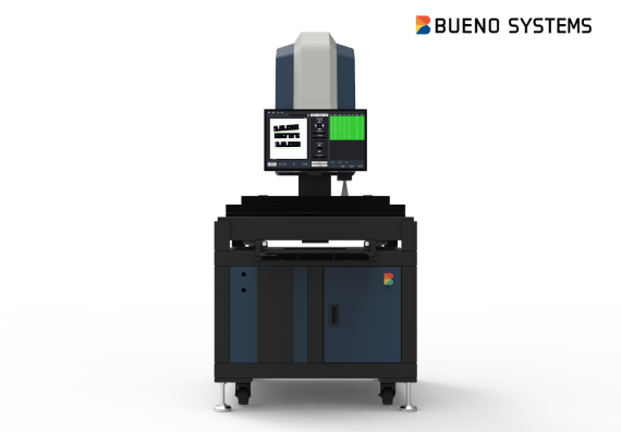
2D Intelligent Optical Recognition Measuring Instrument
▍Advantages and Features Measure multiple sizes simultaneously within seconds. This saves more manpower and working time. AI automated recognition. This improves the measuring efficiency of an enterprise greatly. Easy operation and burden-free. Anyone can obtain stable and precise measuring results. ▍Key Core Technology of AL-2AT Service Automatic focus adjustment with special optical lens / Fuzzy point-capturing function / Fuzzy point-capturing function Fuzzy point-capturing function / Fuzzy point-capturing function ▍Applications of AL-2AT Series First RD work and initial product inspection / IPQC and sampling inspection / OQC inspection / IQC inspection ▍Diversified Measurement Usage Applicable for: Measurements of gaskets and sealing parts, connectors, springs, engineering plastic parts, fabricated parts for precision machinery, automobile and aerospace parts, stamping parts, gears, bearings, hardware fasteners, die cast pieces, etc.
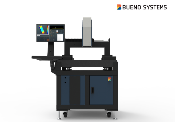
Non-contact 3D Surface Profile Optical Measuring Instrument
▍Advantages and Features Acquire 3D data on work piece surface rapidly within minutes, improving the measuring efficiency of an enterprise greatly. Exclusive optical structure and core algorithm are used to combine 15 measuring functions in one device for satisfying the multiple measuring requirements of enterprises. Non-contact measuring does not damage products, so there is no need for increase of costs. High precision linear scale mobile platform can be applied in measurement of large scale objects. Easy operation and burden-free, anyone can obtain stable and precise measuring results. Measurement data digitization provides clients with complete database collection. ▍Applications of AL-3AT Series First RD work and initial product inspection / IPQC and sampling inspection / OQC inspection / IQC inspection ▍Diversified Measurement Usage Applicable for: Measurements of gaskets and sealing parts, connectors, sheet metal parts, springs, mold, engineering plastic parts, fabricated parts for precision machinery, automobile and aerospace parts, extrudate , stamping parts, gears, bearings,hardware fasteners, die cast pieces, film thickness measuring, etc.
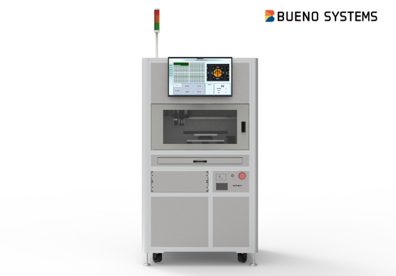
Intelligent Optical Wafer/Chip Surface Defect and Height Variation Detection
▍Providing precise optical inspection and analysis for defects generated during semiconductor wafer fabrication processes. Measurement Techniques: → Utilizing an autofocus microscope module combined with an XYZ axis displacement platform (integrated with optical ruler) for aerial imaging, capturing surface images of wafers/chips. → Employing image contrast and AI image depth learning techniques to detect defects as required, reducing occurrences of overkill and underkill. → Clear and detailed AI determination results, including defect types, coordinates, areas, and quantities on wafers, with comprehensive data integration. → Customizable tolerance settings for automatic sorting of OK/NG parts, calculating defect area sizes, defect quantities, and annotating defect positions, with potential for automation integration to enhance detection efficiency.
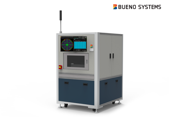
Intelligent Automatic Wafer Thickness Measurement Equipment
▍Multi-functional wafer measutement instrument, using upper and lower high-precision white light conjugate focal sensors for measuring wafer thickness, curvature, etc. → Addressing the thickness monitoring requirements for semiconductor wafer grinding, thinning processes, CVD deposition, epitaxy, and film growth processes. → Provides precise measurement and analysis of wafer bow, curvature, and thickness uniformity generated during processing. → Utilizes non-contact sensors with high-precision displacement platforms for full-plane scanning. → Work orders can be provided using barcode method, automatically read barcode according to customer fotmat, and automatically load measurement parameters for measurement. → The seneor head adopts a non-contact high-precision dual-head sensor. → Customizable number of measurement points, built-in sofware point path, including 5 points, 9 points, 37 points, and custom points, to achieve multi-point measurement information; the system can also read WAFER ID information from the wafer.
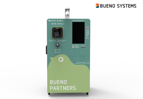
Reverse Vending Machin
▍Condensing tedious operations into one device. → Instant classification with dedicated inlet, no manual sorting required. → Material identification for designated materials only. → Simulating delivery scenarios, use AI image recognition to excluding exceptional case. → Shortening the recycling process, compressing PET bottles to maximize storage space. → Reducing manual work, deliver recyclables to cleaning facility directly. → Constructing IoT database and integrating information.